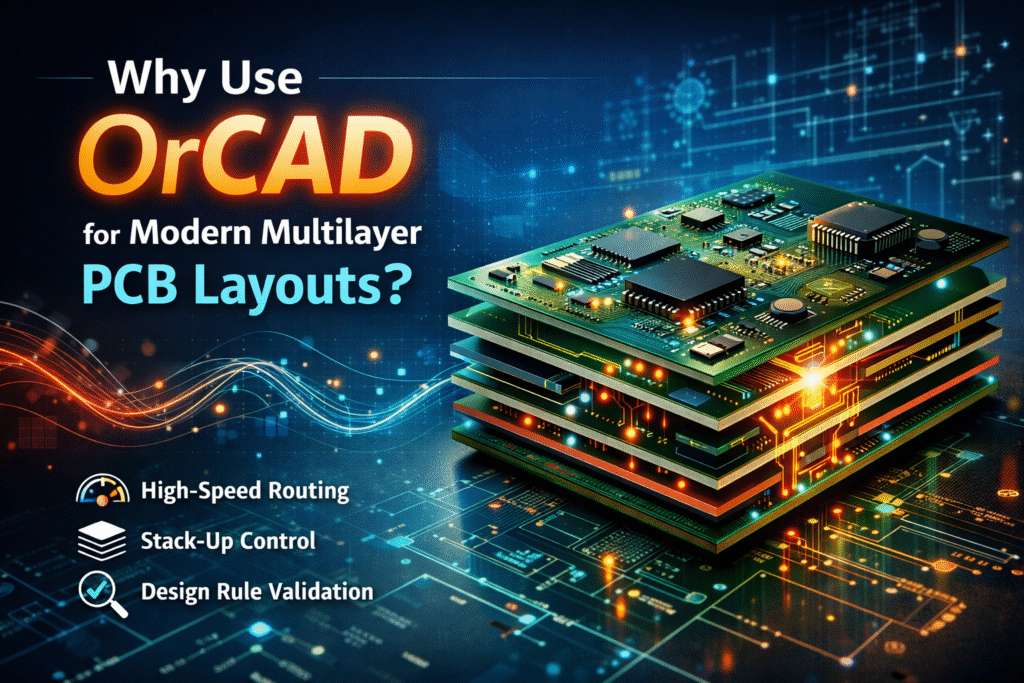
Modern electronics are becoming smaller, faster, and more complex than ever before. From high-speed communication devices to advanced industrial systems, today’s hardware demands highly optimized multilayer board designs. In this evolving landscape, selecting the right PCB design environment plays a critical role in ensuring performance, reliability, and manufacturability. Many engineers rely on tools like OrCAD PCB Designer to streamline layout workflows, manage dense routing, and support advanced stack-up configurations. But what makes such platforms especially valuable for modern multilayer PCB layouts?
This article explores the technical, strategic, and workflow-related reasons behind adopting advanced PCB design systems for multilayer boards, while aligning with current 2025 best practices in electronics development and search-driven content standards.
The Growing Complexity of Multilayer PCB Layouts
Multilayer PCBs are no longer limited to high-end industrial applications. Even mid-range consumer electronics now require four, six, eight, or more layers to support signal integrity, EMI control, and compact mechanical constraints. As data speeds increase and device footprints shrink, board layouts must accommodate:
- High-speed differential routing
- Controlled impedance traces
- Power distribution networks (PDNs)
- Ground plane optimization
- Thermal management strategies
- Dense component placement
Traditional layout approaches often struggle under these demands. Engineers require intelligent routing systems, real-time design rule checks, and advanced visualization features to manage complexity efficiently.
This is where structured PCB design platforms become essential. A professional environment such as OrCAD PCB Designer supports multilayer workflows through automation, constraint-driven routing, and integrated verification processes.
Managing Layer Stack-Up with Precision
One of the most critical aspects of multilayer PCB design is stack-up configuration. The arrangement of signal, power, and ground layers directly influences performance characteristics such as signal integrity and electromagnetic compatibility.
Modern PCB tools provide stack-up editors that allow engineers to:
- Define dielectric materials and thickness
- Control impedance parameters
- Adjust copper weights
- Visualize signal return paths
- Simulate high-speed layer behavior
Accurate stack-up planning reduces late-stage redesign risks and improves manufacturing predictability. With growing demand for high-frequency applications in 5G, IoT, automotive electronics, and aerospace systems, stack-up control is no longer optional—it is foundational.
High-Speed Design Requirements
In 2025, high-speed digital design is no longer confined to niche industries. Even consumer-level electronics require signal performance optimization. PCB layouts must account for:
- Crosstalk mitigation
- Length matching
- Differential pair management
- Via stubs and back drilling
- Return path continuity
Advanced PCB design platforms integrate constraint managers that allow engineers to define electrical rules before routing begins. This proactive approach reduces errors and ensures compliance with performance standards.
When routing multilayer boards, intelligent auto-interactive routing significantly improves productivity while maintaining precision. This balance between automation and manual control is essential in modern PCB design workflows.
Efficient Handling of Dense Component Placement
Board real estate is shrinking. Engineers are constantly challenged to fit more components into smaller footprints while maintaining signal quality and thermal balance.
Modern multilayer design environments assist by offering:
- Real-time clearance checks
- 3D visualization for mechanical fit
- High-density interconnect (HDI) support
- Microvia and blind/buried via handling
- Dynamic copper pour management
Such capabilities reduce manual iteration and enhance layout accuracy. The ability to visualize board layers and component interactions in 3D has become particularly valuable for avoiding mechanical conflicts early in development.
Integrated Design Rule Checking and Validation
Error detection during layout is one of the most important productivity features in PCB design. Real-time design rule checking (DRC) ensures:
- Proper spacing between traces
- Compliance with fabrication tolerances
- Signal class consistency
- Electrical clearance safety
Instead of identifying issues during final review, engineers can correct problems immediately. This reduces redesign cycles and aligns with modern lean development methodologies.
To better understand how multilayer PCB tools address layout complexity and rule-driven workflows, you can explore this in-depth analysis on how OrCAD PCB Designer handles multilayer PCB designs easily, which explains practical approaches to managing structured design constraints and improving board-level accuracy. This discussion further highlights how modern PCB environments simplify multilayer board management, especially for complex and high-density layouts.
Signal Integrity and Power Integrity Optimization
As switching speeds increase, signal and power integrity analysis must be integrated into the design process. Poor routing decisions can result in reflections, ringing, or noise coupling.
Modern multilayer PCB tools help designers:
- Analyze impedance matching
- Optimize decoupling capacitor placement
- Control return paths
- Minimize loop areas
- Improve plane segmentation
These features are critical for applications operating at gigahertz frequencies. Proper power distribution network (PDN) design ensures stable voltage delivery across multiple layers, especially in boards with high current demands.
Collaboration and Workflow Integration
Engineering teams rarely work in isolation. Modern PCB development involves collaboration between:
- Schematic designers
- Layout engineers
- Mechanical teams
- Manufacturing partners
- Compliance reviewers
Integrated design platforms facilitate version control, annotation synchronization, and cross-domain communication. When schematic changes occur, layout updates can be managed systematically, reducing risk of inconsistencies.
The ability of OrCAD PCB Designer to maintain synchronization between schematic and layout stages contributes to more reliable board development cycles.
Manufacturing-Ready Output and Documentation
Design success is incomplete without manufacturability. Multilayer boards must be fabricated with precision, and design files must clearly communicate specifications.
Modern PCB layout tools generate:
- Gerber files
- ODB++ outputs
- Drill data
- Assembly drawings
- Pick-and-place files
Advanced manufacturing checks ensure that trace widths, via sizes, and annular rings meet fabrication standards. By integrating design-for-manufacturing (DFM) considerations early, engineers reduce costly production delays.
Thermal Management in Multilayer Designs
Thermal control is increasingly important in compact electronics. High-performance processors and power devices generate significant heat, which must be dissipated effectively.
Multilayer boards provide opportunities for:
- Thermal vias
- Heat spreading planes
- Copper balancing
- Strategic component placement
PCB design platforms support thermal-aware routing and plane analysis, allowing engineers to simulate and refine heat distribution paths. This is especially valuable in automotive, industrial, and embedded systems applications.
Scalability for Future Design Demands
Technology evolves rapidly. Tools used today must remain adaptable for tomorrow’s requirements. Scalable PCB design environments accommodate:
- Increasing layer counts
- Higher frequency signals
- Advanced materials
- Miniaturized components
- AI-assisted routing features
The adaptability of OrCAD PCB Designer makes it suitable for engineers working on both moderate and highly complex multilayer projects. Scalability ensures long-term usability without constant migration to new platforms.
Alignment with Engineering Trends
Current industry discussions emphasize efficiency, automation, and reliability. PCB designers are expected to:
- Reduce turnaround time
- Increase first-pass success rates
- Improve simulation-driven design
- Minimize manual rework
- Enhance cross-functional collaboration
Modern PCB platforms respond to these demands through constraint-driven workflows and intelligent routing algorithms.
Additionally, sustainability considerations are influencing design strategies. Efficient multilayer routing reduces material waste and manufacturing defects, indirectly contributing to greener electronics production.
Why Engineers Continue Choosing Structured PCB Platforms
The preference for professional PCB design environments is driven by several consistent advantages:
- Improved layout accuracy
- Reduced error rates
- Enhanced signal performance
- Streamlined manufacturing output
- Better team collaboration
- Support for advanced stack-up management
Multilayer PCB layout is no longer simply about placing traces across several copper layers. It requires holistic design thinking that integrates electrical performance, thermal behavior, mechanical fit, and manufacturability.
By providing comprehensive design capabilities within a unified workflow, tools like OrCAD PCB Designer empower engineers to meet modern expectations confidently.
Final Thoughts
The increasing complexity of electronic systems demands more than basic layout tools. Modern multilayer PCB layouts require precision, automation, real-time validation, and scalable architecture support. From stack-up planning to high-speed routing and manufacturing output, every stage must be optimized for performance and reliability.
Choosing a structured PCB design platform ensures engineers can handle dense component placement, signal integrity challenges, and advanced power distribution networks effectively. As electronics continue to evolve in 2025 and beyond, the importance of intelligent multilayer PCB design solutions will only grow.
For teams aiming to deliver high-performance hardware with reduced development cycles, leveraging advanced capabilities in environments such as OrCAD PCB Designer represents a strategic and future-ready decision.